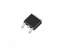
APM3055L
____________________________________
Features
@ VGS=4.5V Super High Dense Cell Design High Power and Current Handling Capability TO-252
ApplicationsSymbol VDSS VGSS ID IDM Drain-Source Voltage Gate-Source Voltage Parameter
Maximum Drain Current Continuous Maximum Drain Current Pulsed
ANPEC reserves the right to make changes to improve reliability or manufacturability without notice, and advise customers to obtain the latest version of relevant information to verify before placing orders. Copyright ANPEC Electronics Corp. Rev. A.6 - Apr., 2002 1 www.anpec.com.tw
Symbol PD Parameter Maximum Power Dissipation TA=100°C TJ TSTG Maximum Junction Temperature Storage Temperature Range TO-252
Symbol Static BVDSS IDSS VGS(th) IGSS RDS(ON) Parameter Drain-Source Breakdown Voltage Zero Gate Voltage Drain Current Gate Threshold Voltage Gate Leakage Current Drain-Source On-state Resistance VSD Dynamic Q gd tON td(ON) tr td(OFF) tf tOFF Total Gate Charge Gate-Source Charge Gate-Drain Charge Turn-on Time Turn-on Delay Time Turn-on Rise Time Turn-off Delay Time Turn-off Fall Time Turn-off Time Diode Forward Voltage


